from solcore import material, si
from solcore.absorption_calculator import search_db, download_db
import os
from solcore.structure import Layer
from solcore.light_source import LightSource
from rayflare.transfer_matrix_method import tmm_structure
from rayflare.options import default_options
from rayflare.structure import Interface, BulkLayer, Structure
from rayflare.matrix_formalism import process_structure, calculate_RAT
from solcore.constants import q
import numpy as np
import matplotlib.pyplot as pltSection 9a: Planar III-V on planar Si, with rear grating
In this example, we will build two structures similar to those described in this paper. These are both triple-junction, two-terminal GaInP/GaAs/Si cells; one cell is planar, while the other has a diffraction grating deposited on the rear of the bottom Si cell to boost its current.
Setting up
As before, we load some materials from the refractiveindex.info database. The MgF\(_2\) and Ta\(_2\)O\(_5\) are the same as the ARC example; the SU8 is a negative photoresist which was used in the reference paper The optical constants for silver are also loaded from a reliable literature source. Note that the exact compositions of some semiconductor alloy layers (InGaP, AlInP and AlGaAs) are not given in the paper and are thus reasonable guesses.
download_db() # only needs to be run onceMgF2_pageid = search_db(os.path.join("MgF2", "Rodriguez-de Marcos"))[0][0];
Ta2O5_pageid = search_db(os.path.join("Ta2O5", "Rodriguez-de Marcos"))[0][0];
SU8_pageid = search_db("SU8")[0][0];
Ag_pageid = search_db(os.path.join("Ag", "Jiang"))[0][0];
MgF2 = material(str(MgF2_pageid), nk_db=True)();
Ta2O5 = material(str(Ta2O5_pageid), nk_db=True)();
SU8 = material(str(SU8_pageid), nk_db=True)();
Ag = material(str(Ag_pageid), nk_db=True)();
window = material("AlInP")(Al=0.52)
GaInP = material("GaInP")(In=0.5)
AlGaAs = material("AlGaAs")(Al=0.8)
GaAs = material("GaAs")()
Si = material("Si")
Air = material("Air")()
Al2O3 = material("Al2O3P")()
Al = material("Al")()Defining the cell layers
Now we define the layers for the III-V top junctions, and the Si wafer, grouping them together in a logical way. In this example, we will only do optical simulations, so we will not set e.g. diffusion lengths or doping levels.
ARC = [
    Layer(110e-9, MgF2),
    Layer(65e-9, Ta2O5),
]

GaInP_junction = [
    Layer(17e-9, window),
    Layer(400e-9, GaInP),
    Layer(100e-9, AlGaAs)
]

tunnel_1 = [
    Layer(80e-9, AlGaAs),
    Layer(20e-9, GaInP),
]

GaAs_junction = [
    Layer(17e-9, GaInP),
    Layer(1050e-9, GaAs),
    Layer(70e-9, AlGaAs)]

tunnel_2 = [
    Layer(50e-9, AlGaAs),
    Layer(125e-9, GaAs),
    ]

Si_junction = [
    Layer(280e-6, Si(Nd=si("2e18cm-3"), hole_diffusion_length=2e-6), role="emitter"),
]

coh_layers = len(ARC) + len(GaInP_junction) + len(tunnel_1) + len(GaAs_junction) + \
               len(tunnel_2)
As for Example 7, to get physically reasonable results we must treat the very thick layers in the structure incoherently. The coh_layers variable sums up how many thin layers (which must be treated coherently) must be included in the coherency_list options.
Planar cell
Now we define the planar cell, and options for the solver:
cell_planar = tmm_structure(
    ARC + GaInP_junction + tunnel_1 + GaAs_junction + tunnel_2 + Si_junction,
    incidence=Air,
    transmission=Ag,
)

n_layers = cell_planar.layer_stack.num_layers

coherency_list = ["c"]*coh_layers + ["i"]*(n_layers-coh_layers)

options = default_options()

wl = np.arange(300, 1201, 10) * 1e-9
AM15G = LightSource(source_type="standard", version="AM1.5g", x=wl,
                    output_units="photon_flux_per_m")

options.wavelengths = wl
options.coherency_list = coherency_list
options.coherent = False
Run the TMM calculation for the planar cell, and then extract the relevant layer absorptions. These are used to calculate limiting currents (100% internal quantum efficiency), which are displayed on the plot with the absorption in each layer.
tmm_result = cell_planar.calculate(options=options)

GaInP_A = tmm_result['A_per_layer'][:,3]
GaAs_A = tmm_result['A_per_layer'][:,8]
Si_A = tmm_result['A_per_layer'][:,coh_layers]

Jmax_GaInP = q*np.trapz(GaInP_A*AM15G.spectrum()[1], x=wl)/10
Jmax_GaAs = q*np.trapz(GaAs_A*AM15G.spectrum()[1], x=wl)/10
Jmax_Si = q*np.trapz(Si_A*AM15G.spectrum()[1], x=wl)/10

R_spacer_ARC = tmm_result['R']

plt.figure(figsize=(6,4))
plt.plot(wl * 1e9, GaInP_A, "-k", label="GaInP")
plt.plot(wl * 1e9, GaAs_A, "-b", label="GaAs")
plt.plot(wl * 1e9, Si_A, "-r", label="Si")
plt.plot(wl * 1e9, 1 - R_spacer_ARC, '-y', label="1 - R")

plt.text(450, 0.55, r"{:.1f} mA/cm$^2$".format(Jmax_GaInP))
plt.text(670, 0.55, r"{:.1f} mA/cm$^2$".format(Jmax_GaAs))
plt.text(860, 0.55, r"{:.1f} mA/cm$^2$".format(Jmax_Si))
plt.xlabel("Wavelength (nm)")
plt.ylabel("Absorptance")
plt.tight_layout()
plt.legend(loc='upper right')
plt.legend(bbox_to_anchor=(1.05, 1), loc=2, borderaxespad=0.)
plt.show()
Database file found at /Users/phoebe/.solcore/nk/nk.db
Material main/Ag/Jiang.yml loaded.
Database file found at /Users/phoebe/.solcore/nk/nk.db
Material main/Ag/Jiang.yml loaded.
Database file found at /Users/phoebe/.solcore/nk/nk.db
Material main/MgF2/Rodriguez-de Marcos.yml loaded.
Database file found at /Users/phoebe/.solcore/nk/nk.db
Material main/MgF2/Rodriguez-de Marcos.yml loaded.
Database file found at /Users/phoebe/.solcore/nk/nk.db
Material main/Ta2O5/Rodriguez-de Marcos.yml loaded.
Database file found at /Users/phoebe/.solcore/nk/nk.db
Material main/Ta2O5/Rodriguez-de Marcos.yml loaded.
Cell with rear grating
Now, for the cell with a grating on the rear, we have a multi-scale problem where we must combine the calculation of absorption in a very thick (compared to the wavelengths of light) layer of Si with the effect of a wavelength-scale (1000 nm pitch) diffraction grating. For this, we will use the Angular Redistribution Matrix Method (ARMM) which was also used in Example 8.
The front surface of the cell (i.e. all the layers on top of Si) are planar, and can be treated using TMM. The rear surface of the cell, which has a crossed grating consisting of silver and SU8, must be treated with RCWA to account for diffraction. The thick Si layer will be the bulk coupling layer between these two interfaces.
First, we set up the rear grating surface; we must define its lattice vectors, and place the Ag rectangle in the unit cell of the grating. More details on how unit cells of different shapes can be defined for the RCWA solver can be found here.
x = 1000

d_vectors = ((x, 0), (0, x))
area_fill_factor = 0.4
hw = np.sqrt(area_fill_factor) * 500

back_materials = [Layer(width=si("250nm"),
        material=SU8,
        geometry=[{"type": "rectangle", "mat": Ag, "center": (x / 2, x / 2),
                   "halfwidths": (hw, hw), "angle": 0}],
    )]
Now, we define the Si bulk layer, and the III-V layers which go in the front interface. Finally, we put everything together into the ARMM Structure, also giving the incidence and transmission materials.
bulk_Si = BulkLayer(280e-6, Si(), name="Si_bulk")

III_V_layers = ARC + GaInP_junction + tunnel_1 + GaAs_junction + tunnel_2

front_surf_planar = Interface("TMM", layers=III_V_layers, name="III_V_front",
                              coherent=True)

back_surf_grating = Interface(
    "RCWA",
    layers=back_materials,
    name="crossed_grating_back",
    d_vectors=d_vectors,
    rcwa_orders=60,
)

cell_grating = Structure(
    [front_surf_planar, bulk_Si, back_surf_grating],
    incidence=Air,
    transmission=Ag,
)
Because RCWA calculations are very slow compared to TMM, it makes sense to only carry out the RCWA calculation at wavelengths where the grating has any effect. Depending on the wavelength, all the incident light may be absorbed in the III-V layers or in its first pass through the Si, so it never reaches the grating. We check this by seeing which wavelengths have even a small amount of transmission into the silver back mirror, and only doing the new calculation at these wavelengths. At shorter wavelengths, the results previously calculated using TMM can be used.
wl_rcwa = wl[tmm_result['T'] > 1e-4] # check where transmission fraction is bigger
# than 1E-4

options.wavelengths = wl_rcwa
options.project_name = "III_V_Si_cell"
options.n_theta_bins = 30
options.c_azimuth = 0.25

process_structure(cell_grating, options, save_location='current')
results_armm = calculate_RAT(cell_grating, options, save_location='current')
RAT = results_armm[0]
Comparison of planar and grating cell
We extract the relevant absorption per layer, and use it to calculate the new limiting current for the Si junction. The plot compares the absorption in the Si with and without the grating.
Si_A_total = np.zeros(len(wl))
Si_A_total[tmm_result['T'] > 1e-4] = RAT['A_bulk'][0]
Si_A_total[tmm_result['T'] <= 1e-4] = Si_A[tmm_result['T'] <= 1e-4]

Jmax_Si_grating = q*np.trapz(Si_A_total*AM15G.spectrum()[1], x=wl)/10

plt.figure(figsize=(6,3))
plt.plot(wl * 1e9, GaInP_A, "-k", label="GaInP")
plt.plot(wl * 1e9, GaAs_A, "-b", label="GaAs")
plt.plot(wl * 1e9, Si_A, "--r", label="Si (planar)")
plt.plot(wl * 1e9, Si_A_total, '-r', label="Si (with grating)")
plt.text(420, 0.55, r"{:.1f} mA/cm$^2$".format(Jmax_GaInP))
plt.text(670, 0.50, r"{:.1f} mA/cm$^2$".format(Jmax_GaAs))
plt.text(860, 0.45, r"{:.1f} mA/cm$^2$".format(Jmax_Si_grating))
plt.legend(bbox_to_anchor=(1.05, 1), loc=2, borderaxespad=0.)
plt.xlabel("Wavelength (nm)")
plt.ylabel("Absorptance")

plt.tight_layout()
plt.show()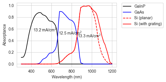
Questions
- Why does the grating only affect the absorption in Si at long wavelengths?
- What is the reason for using the angular redistribution matrix method, rather than defining an RCWA-only structure (
rcwa_structure)?